
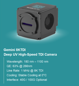
Every UV camera datasheet leads with a quantum efficiency figure, and every supplier presents it as evidence of sensitivity. Buyers who compare those numbers directly, however, frequently end up with a camera that performs poorly on their own samples. The reason is not dishonesty. It is that a single peak value, measured under favourable conditions and quoted without context, says very little about whether a defect will be visible at the exposure time the application actually allows.
For anyone selecting an instrument, the useful question is narrower and more practical: at my wavelength, at my exposure, and at my noise budget, will this sensor produce a defect signature I can trust? Answering it requires reading quantum efficiency together with three other specifications, and understanding how they interact.
What Quantum Efficiency Actually Measures
Quantum efficiency is the fraction of incident photons that produce a measurable signal in the sensor. A value of 48% at 365 nm means that slightly fewer than half of the ultraviolet photons reaching the sensor contribute to the image; the rest are absorbed without generating charge, reflected at a coating interface, or lost in the conversion chain. In the visible band, modern backside-illuminated sensors routinely exceed 90%. In the ultraviolet, the same device may fall to a third of that, because UV photons are absorbed very close to the surface where interface states and passivation layers interfere.
This is why UV sensitivity is an engineering problem rather than a purchasing one. Getting high quantum efficiency below 300 nm requires dedicated backside processing, anti-reflection coatings tuned for short wavelengths, and careful control of the surface dead layer. Two sensors built on the same underlying silicon can differ by a factor of two in the UV.
Peak Value Versus In-Band Value
The first trap is comparing a peak figure with an in-band figure. A camera quoted at 95% peak quantum efficiency is likely quoting a value near 500 to 600 nm, which is irrelevant to an application running at 266 nm. What matters is the curve at the illumination wavelength, and whether that curve is measured or modelled.
The second trap is the shape of the curve near the band edge. A sensor that holds 60% at 280 nm but drops to 15% at 250 nm is not a deep-UV camera in any practical sense; it is a visible camera with a usable near-UV shoulder. Applications that mix illuminators, for example a 365 nm alignment channel with a 266 nm inspection channel, need the curve to be adequate at both points, not excellent at one.
Quantum Efficiency Alone Does Not Produce Contrast
Contrast is signal divided by noise, and quantum efficiency only addresses the numerator. A camera with 65% quantum efficiency and 8 electrons of read noise will lose to a camera with 50% quantum efficiency and 1 electron of read noise whenever the signal is a few dozen photons. In dark-field wafer defect inspection, where a sub-micron particle may scatter only a handful of photons into the collection aperture per microsecond, this is the normal operating regime rather than an edge case.
Dark current enters the same calculation from a different direction. It is negligible for a 200-microsecond exposure and dominant for a two-second integration. Systems that combine a fast scan with periodic long-exposure review therefore need the sensor to be good at both, which usually means active cooling rather than a passive heatsink.
The practical consequence is that quantum efficiency should always be requested together with the noise floor at the intended operating temperature, not at a generic 25 degrees Celsius. A specification sheet that quotes read noise without stating the sensor temperature is telling you something, but not something you can design around.
Why the Wavelength-Specific Design Matters More Than the Sensor Generation
It is tempting to assume that a newer sensor generation automatically wins in the UV. In practice, the UV performance of a camera is set by choices made around the die as much as by the die itself: window material and its transmission curve, the sealing approach, the coating stack, and the way the sensor is thermally anchored. A well-integrated camera built on a mature sensor often outperforms a poorly integrated one built on a newer die.
This is the reasoning behind specifying a camera for the band rather than for the brochure. A sensor with 48% quantum efficiency at 365 nm, a global shutter, and a thermal design that holds its noise floor across a shift will beat a nominally more advanced device that was never characterised below 400 nm. The same logic applies one band down, where deep-UV optimisation and cooling technology matter more than pixel count.
A Short Vendor Question List
Four questions separate a real specification from a marketing one. Is the quantum efficiency curve measured on production units or on a selected sample? At what sensor temperature were the noise figures taken, and does the camera hold that temperature at the ambient temperature of my tool? What is the exposure-time penalty for reaching the quoted frame rate at full resolution? And what happens to fixed-pattern structure after several hours of operation, when thermal gradients have fully developed?
Answers to those four questions, rather than the headline number, determine whether a UV camera will detect the defects it is bought to detect. Anyone comparing options in detail will find a structured comparison in this guide to Choosing the Right UV Camera for Semiconductor Inspection, which walks through the band-by-band trade-offs and the camera characteristics each band demands.
Conclusion
Quantum efficiency is a necessary specification and a poor headline. Read in isolation it flatters sensors that cannot deliver contrast at realistic exposure times, and it undersells sensors that were designed for a specific band. The purchasing decision improves dramatically once quantum efficiency, read noise, dark current, and thermal stability are evaluated as one system, at the wavelength and temperature the tool will actually use.